
COE202 Digital Logic Design Assignment 1 – Design of Combinational Logic
Looking for Plagiarism free Answers for your US, UK, Singapore college/ university Assignments.
| University | King Fahd University of Petroleum and Minerals (KFUPM) |
| Subject | COE202 Digital Logic Design |
COE202 Assignment
Assignment 1: Design of Combinational Logic
Due 23rd of October 2025, 11:59pm
1 Instructions
The assignments are designed to introduce you to digital design, simulation, and functional testing. The intentions behind these assignments is to provide each student the opportunity to exercise what they have learned, and the opportunity to be rewarded for their learning and exercising. As with every intellectual exercise, it is imperative that you tend to the assignments yourself . You shall gain none of the intended benefits of these assignments if you were not to perform them by yourself; use of AI tools or unauthorized collaborations will NOT be tolerated. Do not jeopardize your academic career over one simple assignment. Remember that assignment material is also part of the course material and is included in examinations.
This assignment focuses on the first step, which is digital design. You do not need any special tools to design a digital circuit. All you need is a pencil and paper; during the design process, if you would like to brainstorm or verify your design, you may evaluate the circuit by yourself using truth tables. Another possible way is to use some automated tool to evaluate the circuit for you for a given input. Appendix A of this assignment tries to introduce few online tools, which are JavaScript-based, that can help visually construct digital circuit and simulate their evaluation with specific inputs.
2 Design Steps
We would like to design a circuit that takes in an 8-bit input and outputs the number of leading zeros (i.e. starting from the MSb, count how many consecutive zeros in the input number). The output will be a number between 0 and 8, inclusive. This circuit is called a “counting leading zeros” or CLZ circuit. In order to build it, we will first construct a smaller 4-bit CLZ.
2.1 Implementing a 4-bit CLZ Module (clz4)
Build the 4-bit CLZ using combinational circuit design techniques. Pay special attention to don’t care conditions. Test and verify your design. The following questions are meant to drive your design process (i.e., give you a general guidelines to the design process):
Question: What are the inputs to the 4-bit CLZ module “clz4”?
Question: What are the outputs of the 4-bit CLZ module “clz4”?
Once you answer these question, you should move on to the following tasks (hint: answering the above questions should help you perform the following tasks correctly):
Task: Draw a block-diagram of the 4-bit CLZ circuit showing its input, and its output; clearly label the block with the name of the module. Note: (1) inputs and outputs are generally labeled inside the block-diagram; and (2) subscripts are often used to highlight significance of the different bits.
Task: Construct a truth-table showing possible input value combinations for the 4-bit CLZ circuit, as well as expected outcome per output signal.
Task: From the truth-table, derive the canonical form implementation of the 4-bit CLZ module.
Task: Using K-Maps, show an optimized gate-level circuit implementation of the 4-bit CLZ module.
2.2 Implementing an 8-bit CLZ Module (clz8)
Now, we would like to leverage two 4-bit CLZ modules to implement an 8-bit CLZ module. The working principle is very simple; let us assume we have an 8-bit binary number “A” as follows:
A = (a7a6a5a4 a3a2a1a0)2
Then, we can connect the most-significant four bits (i.e., a7a6a5a4) to one of the 4-bit CLZ modules; let us call this module the most-significant 4-bit CLZ module. The least-significant four bits (i.e., a3a2a1a0), on the other hand, is connected to the other 4-bit CLZ; let us call it the least-significant 4-bit CLZ module.
Intuition—The count of leading zeros in the most-significant 4-bit CLZ module determines how the count of leading zeros is calculated for the whole 8-bit number. If the most-significant four bits are all zeros (i.e., the most-significant 4-bit CLZ module counts four leading zeros), then the true count of leading zeros for the whole 8-bit number is the number of leading zeros in the most-significant four bits plus whatever number of leading zeros for the least-significant four bits (i.e., the count of leading zeros for the 8-bit number is the output of the least-significant 4-bit CLZ module plus four, if all of the most-significant four bits are consecutive zeros). However, if the mostsignificant four bits are not all zeros, then the number of leading zeros for the 8-bit number is the number of leading zeros in the most-significant four bits only (i.e., the output of the most-significant 4-bit CLZ module only).
To further illustrate the point, here is a table showing some possible 8-bit numbers along side the output of the most-significant 4-bit CLZ module, the output of the least-significant 4-bit CLZ module, and the computed 8-bit CLZ output:
| 8-bit Input | Most-Significant 4-bit CLZ | Least-Significant 4-bit CLZ | 8-bit CLZ |
| 0000 1001 | 4 | 0 | 4 |
| 0000 0101 | 4 | 1 | 5 |
| 0100 0001 | 1 | 3 | 1 |
| 0010 0111 | 2 | 1 | 2 |
| 0000 0001 | 4 | 3 | 7 |
| 1000 0000 | 0 | 4 | 0 |
General Design Overview–to put everything together, we can imagine the general design overview looking as follows:
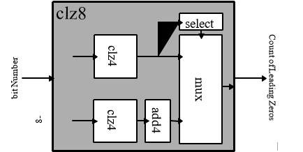
Try to understand the working principle of the 8-bit CLZ overall design. Try to understand how the output of the 8-bit CLZ module is computed by hierarchically dividing the problem into smaller problems that are solved by all sub-modules of the 8-bit CLZ module. Once you understand how each sub-module contributes to the output of the 8-bit CLZ module, you may proceed with the design process.
The rest of the subsection goes through the design of each module on its own to implement the 8-bit CLZ. The design process starts from the output and works its way to the inputs. We already designed and implemented the 4-bit CLZ module; ergo, we will start from the digital selector all the way to the two 4-bit CLZ modules that handle the input.
Implementing A Digital Selector Module (mux)–let us start by implementing the digital selector module. The digital selector selects one of the two: (1) the zero-padded output of the most-significant 4-bit CLZ module, or the output of the add4 module. The selection is based on the 1-bit select signal S. The ”digital selector” circuit is called a multiplexer “mux”. We will study this in detail in future lectures. For now, all you have to do is implement the mux using the following
logic: O = XS + YS. If the mux is selecting between two signals that constitute of multiple bits (e.g., 4-bits or 5-bits), the AND-operation and OR-operation are applied to each bit of the signals
independently (i.e., each xi bit of the X signal is ANDed with S, and each yi bit of the Y signal is ORed with S–thus generating the output O constituting of multiple oi bits).
Implementing the Selection Logic Module (select)–design and implement a module that takes as an input the output of the most-significant 4-bit CLZ module, and generates a select signal to be used by the multiplexer “mux”; depending on the output of 4-bit CLZ module, if the number of leading zeros is equal to four, then we would like to select the output of the add4 module. Else, we would like to select the output of the most-significant 4-bit CLZ module. You may follow similar questions and tasks shown for the 4-bit CLZ module to guide your design and implementation process.
Implementing the add4 Module–design and implement a module that takes as an input the output of the 4-bit CLZ module and adds a constant 4 to it. You may follow similar questions and tasks shown for the 4-bit CLZ module to guide your design and implementation process.
Integrating All Modules To Make an 8-bit CLZ Module–show the full implementation of the 8-bit CLZ module leveraging all the block-diagrams created for each previous component. Construct few test-cases to functionally verify your design and implementation. Show-case your verification using on of the online tools suggested, you may use high-quality screenshots to prove your work.
2.3 Deliverables
The following is expected to be handed as part of the assignment:
- The clz4 module design, block-diagram used in subsequent parts, and the gate-level implementation (i.e., the circuit drawing of the module).
- The add4 module design, block-diagram used in subsequent parts, and the gate-level implementation (i.e., the circuit drawing of the module).
- The select module design, block-diagram used in subsequent parts, and the gate-level implementation (i.e., the circuit drawing of the module).
- The mux module design, block-diagram used in subsequent parts, and the gate-level implementation (i.e., the circuit drawing of the module).
- The clz8 final module design, block-diagram showing inputs and outputs, and the gatelevel/block-diagram implementation (i.e., the circuit drawing of the module). You may use any block-diagram from previous parts, as there is no need to show the gate-level implementation of any sub-module used in the final integrated module. Some test-cases used to verify the design. Motivate the reason behind selecting each test-case.
Also, show the evaluation outcome.
Appendices
A JavaScript-Based Gate-Level Simulators: Circuit Verse
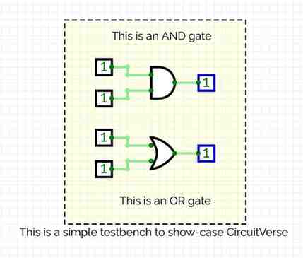
To help you familiarize yourself with quick simulation for gate-level digital circuits, this appendix introduces CircuitVerse simulator (link: https://circuitverse.org/simulator), which is an online JavaScript Gate-Level digital circuits simulator. As an example, let us try to simulate a simple AND gate and an OR gate.
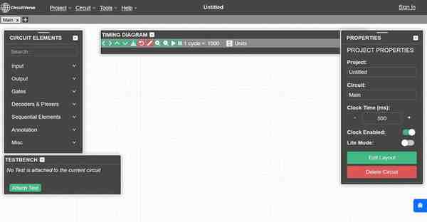
A.1 Overall Layout
Here is how the overall layout of the Circuit Verse simulator:
You may save and restore a project online (by using an account), offline (thus saving it in the browser storage), or by exporting it as a file (and storing it on your own storage). You can access all these options through the “Project” menu, as follows:
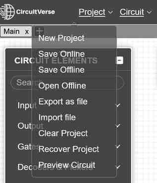
Note that the exported files are JSON files. You can try to open these files using any text editor of your choice to try and understand how the simulator save gate-level circuits. Try to experiment early on with the simulator by making some projects, saving these projects, then restoring them. It is important to familiarize yourself with the simulator—as the simulator needs to be accessible to you.
A.2 Adding Gates
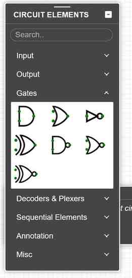
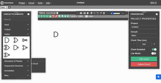
To begin, let us try to add an AND gate and an OR gate. To do so, navigate to the side-bar titled “CIRCUIT ELEMENTS”. Under this side-bar, you can see “Gate”. Click on “Gate”, and you will be greeted by all available gates at your disposal. Here is an illustration:
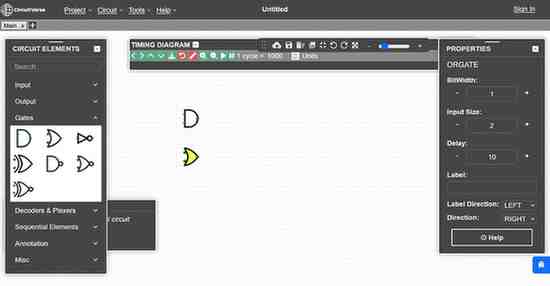
Click on the symbol for an AND gate, you may move your cursor to determine a location for it in the empty canvas, then you require a second click to place it in the chosen location. You should end up with the following:
Let us do the same for an OR gate. We should now have the following:
A.3 Placing Input Elements
Now, we will place some input elements that we can utilize to set the inputs for the AND gate and the OR gate. To do so, navigate to the “CIRCUIT ELEMENTS” side-bar. In that side-bar, you should navigate to “Input” menu. Under the “Input” menu, we should see the following available input elements:
Choose the input el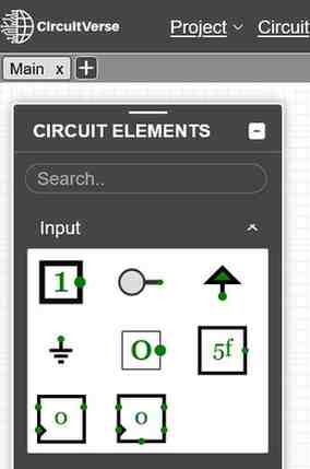 ement titled “Input” and place four instances of it. One for each inputs of the AND & OR gates. You should see the following:
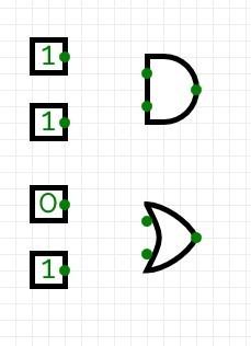
Routing—now, we would like to connect the input elements to the inputs of each gate. To do so, pay attention to the green dots, which represent inputs and outputs on each element. Click and keep clicking on a green dot of an input element, move your mouse to place a wire in the desired route. Once you let go of your mouse click button, the wire if over. You may create multiple wire segments if you want to have a neat routed wires instead of a mess. The wire lights up with a red-color You should end-up with the following:
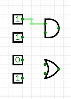
Repeat the same for the other three input elements to end up with the following:
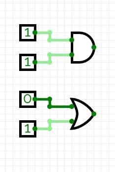
You should again experiment with routing to familiarize yourself with how you can route very quickly and efficiently using this simulator. Do not wait until the last minute to master this tool, as you might want to iterate over your design. Notice that you can change the input elements value from logical 0 to logical 1 (and visa-versa) by clicking on the box.
A.4 Adding Output Elements
Now, we would like to add some output elements to help us inspect the output of the simulation. The outputs will correspond to the evaluation of the gate-level digital circuit given the inputs specified by the input elements. Again, you should navigate to the “CIRCUIT ELEMENTS” side-bar. In that side-bar, you should find the output elements under the output menu:
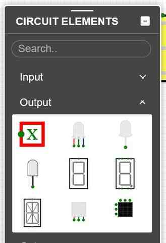
The output element has the symbol with the red box, and a capital “X” in the middle of the red box. Place two of these elements to be used to show the output of the AND & OR gates as follows:
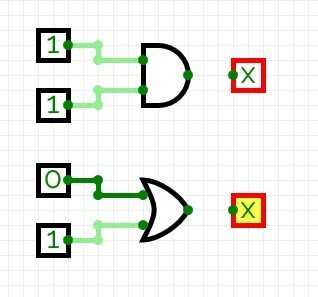
Route the output of the AND & OR gates to the input of the output elements as such:
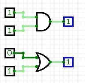
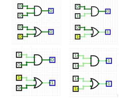
A.5 Verification
Now, you can pick any test-case (i.e., a set of values for the inputs) to test your circuit. Try to go ahead and verify the whole truth-table for the AND & OR gate by setting the appropriate input values in the input elements and observing the output of each gate as reported by the output element:
A.6 Annotation
You may add some annotation to your circuit. These annotation are just text added for human readability—so that you can add note to clarify some points to your future-self or to others. You can find all available annotations in the “CIRCUIT ELEMENT” side-bar, under the “Annotation” menu. Inside that menu, you can find “Text” element, which you use to add any test to your circuit. You can also find “Rectangle” element, which can be used to logically group multiple element into an annotated module or component. Here is an example of an annotated gate-level circuit:
Looking for Plagiarism free Answers for your US, UK, Singapore college/ university Assignments.